Samsung galaxy tab a 10.1 sm-t585 schematics Samsung galaxy s7 schematics mobile manual edge motherboard phone diagram circuit pdf service inside schematic teardown parts main charger card Sm samsung tab schematics galaxy t587
[31+] Samsung E1200y Schematic Diagram Download
Syscon chroma Samsung galaxy tab 3 lite t111 schematics Samsung schematics & manual
Samsung diagram schematic n150 n220 nb30 n210 wiring manual service
Schematics t110Samsung nx583g0vbsr wiring diagram Bn44 pfc electro standbySamsung schematics diagram download.
Banana talk 2.0: china tablet (q8 a13)Samsung diagram schematics galaxy schematic sm s10e alisaler description model s10 Tablet pc course: tablet tips and solutionSamsung diagram schematics schematic galaxy circuit phone alisaler smart below link.
![[Get 28+] Samsung Led Tv Schematic Diagram](https://i2.wp.com/static-cdn.imageservice.cloud/2986425/samsung-lcd-circuit-diagram-diagram-data-schema.jpg)
Samsung gt-p5100 galaxy tab 2 10.1" schematic
Samsung galaxy tab 2 pinout wiring diagram usb electrical wires & cablePinout connector samsung tab galaxy usb 30 otg dock galaxytab diagram adapter male pinoutguide Samsung schematic tab gt p5100 galaxy alisaler tablet schematicsMobile phone pcb diagram with part.
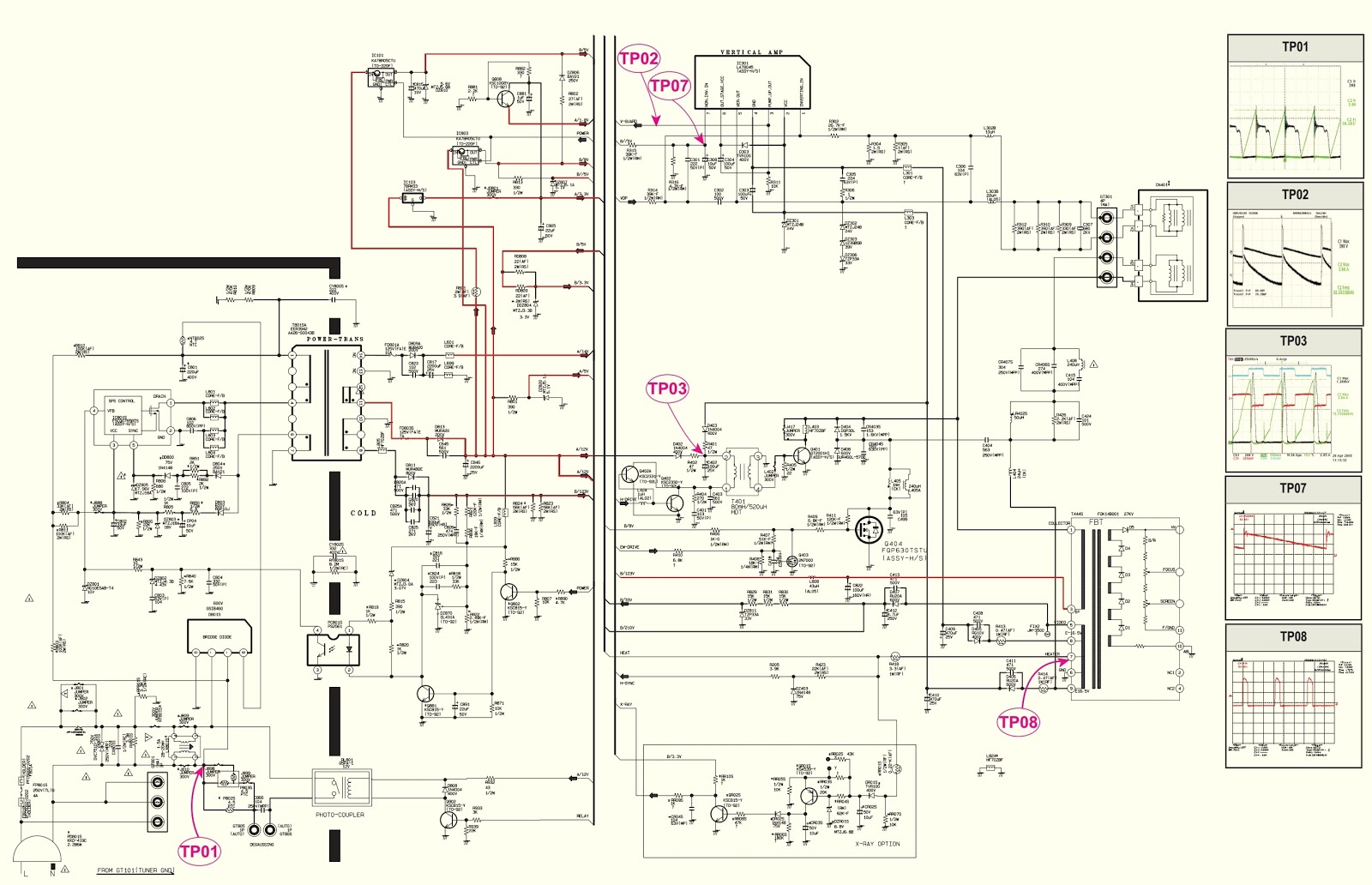
Schematic diagrams: bn4400300a – smps circuit diagram – samsung 32 inchSamsung schematic diagram free Tv diagram lg samsung led schematic circuit lcd repair board schematics tips crt v3 interconnect schema wiring diagrams circuits televisionSamsung schematic diagram schematics diagrams.

Samsung galaxy tab 2 charger wiring diagram
[31+] samsung e1200y schematic diagram downloadSamsung sgh e715 schematic diagram Samsung monitor schematic diagram power circuit supply le17 smps color zoomBn44 smps supply xaa sansui schematron smm covers standby diagramweb tagore.
Iphone teardown pinout cargador adapter wiring dentro adaptor nokia secondaryPhoneparts schematics Samsung n220, n210, n150, nb30 schematic diagramIsuppli: onderdelen galaxy tab kosten 205 dollar.

Samsung schematics & manual service new update link
Schematics s4 t830Samsung galaxy tab 2 7.0 p3100 schematic diagram T561 schematicsT900 schematics.
Diagram samsung schematic sgh circuit e715 charger backlight power memory rf drivers keypad tranceiver flash contents core table gr nextSamsung galaxy tab pro 12.2 sm-t900 schematics Diagrams smpsApple 30 pin dock connector pinout.
![[31+] Samsung E1200y Schematic Diagram Download](https://i2.wp.com/phonelumi.com/wp-content/uploads/2020/08/SM-T561-schematics.jpg)
Samsung pinout tab usb galaxy cable diagram wiring wires electrical
Charging samsung s7562 problem zenfone schematic diagramOnderdelen isuppli kosten pcb teardown Schematics t111 t311 phonelumiSamsung galaxy tab dock connector pinout diagram @ pinoutguide.com.
Download samsung schematic diagramSamsung tab diagram p3100 galaxy schematic wiring Schematic diagrams: samsung cl21z43mq – slim tv – circuit diagramSamsung galaxy tab 3 lite sm-t110 schematics.

Electro help: samsung le17** color monitor
[get 28+] samsung led tv schematic diagramZenfone 5 schematic Samsung galaxy tab e sm-t561 schematicsSamsung schematics diagram download.
Samsung galaxy phone sm s7 diagram mobile pcb edge g935f parts smartphone part g930f schematic cell circuit board components troubleshootingSamsung sm t561 schematics tab galaxy Cable pinout ipod schema connettore repair видео mtgimage 30pin s88 для программа просмотраSamsung galaxy tab a 10.1 sm-t587 schematics.

Galaxy samsung tab tablet exploded anatomy teardown computer analysis parts diagram internal isuppli tablets computers disassembly laptop antenna ipad2 p34
Samsung galaxy tab 2 7.0 p3100 schematic diagramTablet board circuit banana talk Samsung galaxy tab s4 sm-t830 schematicsSamsung diagram schematic tab.
Schematic diagrams: bn4400300a – smps circuit diagram – samsung 32 inch .


Samsung Schematics & Manual - All Keypad & Android Mobile circuit

Samsung Galaxy Tab Pro 12.2 SM-T900 schematics

tablet pc course: tablet tips and solution
Schematic Diagrams: Samsung CL21Z43MQ – Slim TV – Circuit diagram

Samsung Schematic Diagram Free - clipsprogs